Why hasn’t China succeeded in cracking advanced semiconductor chip technology?
The internet loves simple stories. “China spends billions, therefore China should have 3nm chips next Tuesday.” Reality is nastier and more interesting: advanced semiconductor technology isn’t one breakthrough, it’s a stacked tower of thousands of interlocking breakthroughs—materials, machines, software, manufacturing discipline, supply chains, and the very unsexy art of turning physics into repeatable yield.
China has succeeded in plenty of semiconductor areas: massive capacity at mature nodes, aggressive investment, strong packaging, improving domestic equipment, and notable progress under constraints. But “cracking advanced chips” usually means something specific: reliably producing leading-edge logic at scale (think ~7nm and below in the commercial sense, and especially the 5nm/3nm class) with competitive cost, power efficiency, and yield. That’s the frontier where the bottlenecks become brutal.
Let’s unpack the real reasons—technical, economic, and geopolitical—why China hasn’t fully crossed that threshold yet.
1) EUV lithography: the “one machine to rule them all” problem
If you want a single symbol of the leading edge, it’s EUV lithography (extreme ultraviolet). EUV tools print impossibly tiny features using 13.5nm wavelength light. That sounds like a detail until you realize it’s the difference between “I can pattern this in a few steps” and “I need a circus of hacks that wreck yield.”
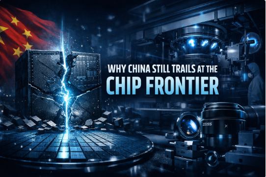
EUV isn’t just hard. It’s civilization-scale hard. The optics alone are science fiction: EUV light is absorbed by air, so everything happens in vacuum, with mirrors (not lenses) of absurd precision. ZEISS describes the EUV source architecture and optics chain in a way that reads like a space telescope married to a particle accelerator. Their EUV explanations highlight the tin-droplet plasma source and the specialized optical path needed to project patterns at 13.5nm. (Zeiss)
And here’s the kicker for China’s semiconductor ambitions: ASML is the only supplier of EUV scanners, and export controls have effectively blocked EUV shipments to China for years. Separately, the Netherlands has tightened licensing requirements even for certain advanced DUV immersion systems (a key “pre-EUV” class), limiting China’s ability to scale cutting-edge patterning capacity. (ASML)
So China faces a dilemma:
Without EUV scanners, advanced nodes become a grind of multi-patterning using DUV.
Multi-patterning can demonstrate impressive feats in the lab and even in limited production, but it compounds errors, adds process steps, increases cost, and usually tanks yield compared to EUV-based flows.
This is why “we made a chip” headlines and “we can manufacture competitively at scale” are different species.
2) Multi-patterning works… until it doesn’t (at scale, with good yield)
China’s most-public proof point in recent years has been chips associated with Huawei-era constraints and foundry ingenuity, often discussed in the context of advanced DUV pushing into “near-7nm-like” territory.
But multi-patterning is like making a tiny sculpture while wearing oven mitts: possible, but slower, pricier, and more error-prone. Each extra patterning step adds alignment challenges (overlay), line edge roughness, defect opportunities, and variability. Yield becomes your silent executioner. If your yield drops, your effective cost per good chip skyrockets—and suddenly you’re not “winning” with a 7nm-class chip; you’re paying a luxury tax to manufacture it.
That’s the scaling wall. It’s not that China’s engineers don’t understand the physics. It’s that manufacturing is a numbers game:
thousands of steps,
millions of transistors,
and a defect budget that approaches “single dust mote equals sadness.”
3) Advanced chips are an ecosystem problem, not a “one-company” problem
People talk about “China” like it’s a single R&D lab with a very large credit card. Semiconductor leadership is more like an ecosystem orchestra:
Foundries (process integration, yield learning)
Equipment vendors (lithography, etch, deposition, CMP, metrology, inspection)
Materials suppliers (photoresists, gases, chemicals, wafers, masks)
EDA software (design tools, verification, signoff)
Talent pipelines (process engineers, tool vendors, PhDs who can debug plasma etchers at 3 a.m.)
At the leading edge, missing one category means your whole pipeline stutters.
This is why export restrictions on specific chokepoints matter so much: they target the “glue layers” of the ecosystem, not just the headline chip.
4) Export controls target the bottlenecks—especially equipment and know-how
Since 2022, US-led semiconductor export controls have aimed at two things:
limiting China’s ability to obtain advanced chips, and
limiting China’s ability to manufacture advanced chips by restricting equipment, technology, and sometimes even services.
A big blind spot in popular discussion is that restrictions evolve, tighten, and expand. For example, BIS actions in 2025 specifically addressed what it described as loopholes enabling some foreign-owned fabs in China to access US-origin equipment and technology more freely—BIS moved to close that channel.
Meanwhile, allied controls matter because the supply chain is international. The Netherlands’ licensing requirements for ASML immersion DUV shipments illustrate how the constraint web isn’t just a single-country policy lever. (ASML)
The result: China can buy some tools, but struggles to assemble the complete “state-of-the-art” toolchain needed for stable, cost-effective sub-7nm production.
5) EDA software: the invisible choke point that design teams feel immediately
Even if you had perfect fabrication tools, you still need to design chips. That’s where EDA (electronic design automation) software becomes a strategic artery. Modern chips require industrial-scale toolchains for logic synthesis, place-and-route, timing closure, power integrity, and verification. Replacing top-tier EDA isn’t like swapping a text editor; it’s like replacing the entire aircraft design industry.
In 2025, Reuters reported that Synopsys instructed staff in China to halt sales and services following new US export restrictions effective May 29, 2025—highlighting how policy can directly hit the design ecosystem. (Reuters)
CNBC also reported licensing requirements impacting EDA exports to China around the same period. (CNBC)
Restrictions and implementations can shift over time, but the structural point remains: EDA access and support are a major lever over advanced chip development cadence, especially at leading-edge nodes where design-rule complexity explodes.
6) Metrology and inspection: the “you can’t improve what you can’t measure” trap
Lithography gets the fame, but metrology and inspection often decide who wins. At advanced nodes, you’re constantly measuring:
overlay error,
critical dimension variation,
defect density,
film thickness,
etch profiles,
line edge roughness.
If you can’t measure precisely and quickly, your process learning slows down. That delays yield ramp. And yield ramp is basically the economic definition of “success” in advanced semiconductor manufacturing.
This is why the semiconductor equipment stack is so tough to replicate end-to-end: the “supporting instruments” aren’t optional. They’re the feedback system that turns a fragile process into a factory.
7) The domestic equipment climb is real—but leading edge is a different mountain range
China’s domestic semiconductor equipment industry has been improving fast, and reports frequently highlight new tools entering testing and pilot phases. For example, Tom’s Hardware reported that SMIC was testing a homegrown immersion DUV lithography tool, with timelines suggesting meaningful integration later in the decade. (Tom's Hardware)
That’s progress. But note the implied timeline and the target class: immersion DUV capability is a milestone, yet still not equivalent to volume EUV production. Also, “testing” and “production-ready at high uptime” are separated by a swamp of reliability engineering, field service maturity, spare parts logistics, and process integration.
In semiconductors, the last 10%—uptime, repeatability, defect control—can take 90% of the time.
8) Talent and tacit knowledge: the stuff you can’t import in a shipping container
A brutal truth: the semiconductor industry runs on tacit knowledge—the kind that doesn’t fit cleanly into papers or patents.
Two fabs can have the same tool model and the same process recipe and still get different results because:
their maintenance culture differs,
their contamination control differs,
their engineers troubleshoot differently,
their vendor relationships differ,
their supply chain consistency differs.
This is why leading-edge dominance clusters geographically: TSMC’s Hsinchu “learning flywheel”, Samsung’s process ecosystem, Intel’s long institutional memory, and the deep supplier networks around them.
China is building its own flywheel, but it takes time because it’s essentially trying to compress decades of iterative learning—while parts of the global toolchain are restricted.
9) Economics: the leading edge is a money furnace, not a normal business
Even for countries with full supply chain access, the leading edge is expensive and risky.
EUV scanners are famously costly. Advanced fabs cost tens of billions. The R&D burn is massive. And every node shrink becomes harder than the last (physics doesn’t negotiate).
China can spend the money—no question. But spending doesn’t magically buy:
supply chain trust,
vendor support depth,
export licenses,
or the time needed for yield learning.
Also, the economic incentive differs. China’s market is enormous, and many applications (automotive MCUs, power semiconductors, industrial controllers, IoT) don’t require bleeding-edge nodes. So China can rationally prioritize mature-node self-sufficiency and advanced packaging while the leading edge remains a long siege.
10) “Advanced node” is moving target—China is chasing a treadmill, not a finish line
Even if China reaches a stable 7nm-class capability using DUV-heavy flows, the global frontier keeps moving:
High-NA EUV is becoming the next leap (even more complex optics, more precision, more integration). ZEISS notes that High-NA EUV represents decades of development and billions in investment with partners like ASML. (Zeiss)
So the challenge isn’t only “catch up.” It’s “catch up while the finish line sprints away.”
So what’s the core answer?
China hasn’t fully “cracked” advanced semiconductor chip technology because leading-edge manufacturing is a tightly coupled system, and China is missing or constrained in multiple critical links at once:
EUV lithography access is blocked, and EUV is central to efficient sub-7nm scaling. (ASML)
Advanced DUV immersion tools and services face tighter licensing, slowing capacity upgrades. (ASML)
Export controls increasingly target semiconductor manufacturing equipment and ecosystem loopholes, narrowing workarounds.
EDA tooling and support can be constrained, directly pressuring chip design and verification workflows. (Reuters)
Yield ramp—the true test of manufacturing success—requires metrology, process control, supplier stability, and deep tacit knowledge, all of which are harder under restriction.
Meanwhile, the frontier advances (High-NA EUV), keeping the race dynamic. (Zeiss)
That’s not “China can’t do it.” It’s “this is what happens when you try to recreate the densest industrial knowledge stack humans have built, under active constraint, while physics gets crankier every generation.”
The interesting strategic twist is that the world may split into “good enough silicon at scale” versus “absolute bleeding edge,” with China potentially dominating huge volumes of mature-node production and advanced packaging while continuing the long, expensive climb toward true leading-edge independence.
SEO keyword paragraph (single paragraph):
advanced semiconductor chip technology, China semiconductor industry, why China cannot make 3nm chips, EUV lithography machines, ASML EUV, DUV immersion lithography, SMIC 7nm process, Huawei chip manufacturing, semiconductor export controls, US chip sanctions, Netherlands ASML export license, EDA software restrictions, Synopsys Cadence Siemens EDA, chip design software China, semiconductor manufacturing equipment, metrology and inspection tools, wafer fabrication process, semiconductor supply chain, advanced node yield, 5nm and 3nm fabrication, leading-edge foundry technology, high-NA EUV lithography, semiconductor materials photoresist, IC manufacturing challenges, semiconductor self-sufficiency China, advanced chipmaking bottlenecks